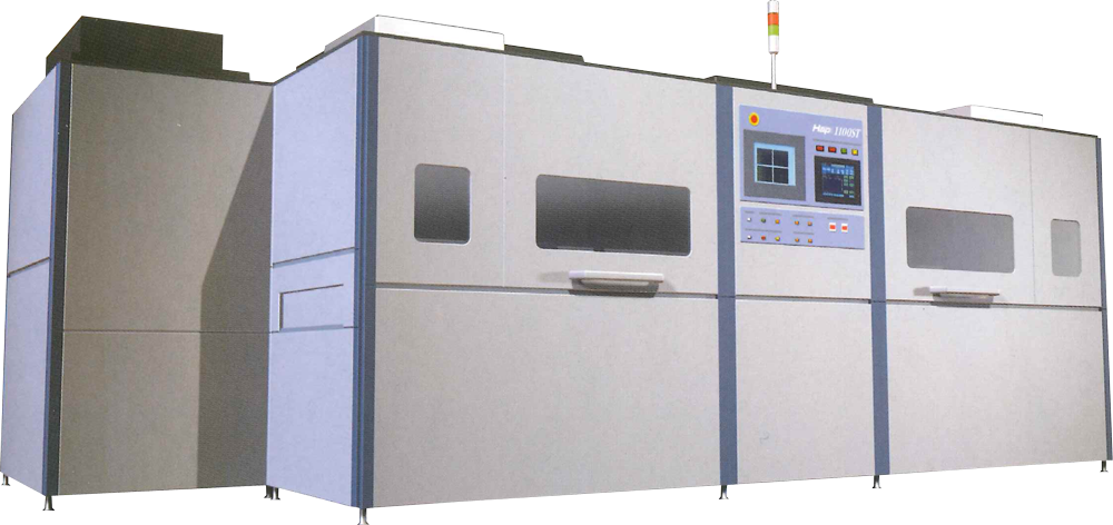
Contact exposure system/Hap1100ST
Exposure system for solder resist mounted with film mask scalingsystem
In addition to the collimated UV light with high-light intensity suitable for SR exposure, the breakthrough “film mask scaling system” is mounted on the one-shot exposure system!
Functions ・ Features
- Solves the problem in the solder resist process
- ■ Film mask to adjust the scale change of PWB
■ High-throughput by high-light intensity
■ Easy control of film mask
■ Stable transfer of plate and weight board
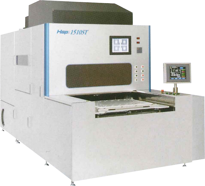
Specifications
- Scaling accuracy
- <10um
- Throughput
- 19.0 sec. + exposure time
- Max. board size
- W610×L510mm
- Light source
- 10kw UV lamp 2 units
- Illuminance intensity
- >80mw/cm2
- Collimated half angle
- ≦2.0°
- Declination angle
- ≦1.5°
- Illumination uniformity
- ≧90%